ECU Firmware extraction is the foundational step in any ECU reverse engineering project. Without a reliable copy of the firmware binary, no meaningful analysis of calibration data, control algorithms, security mechanisms, or potential defeat devices can take place. Yet the method by which you extract that firmware profoundly affects what you obtain, how long it takes, what equipment you need, and whether the ECU survives the process intact.
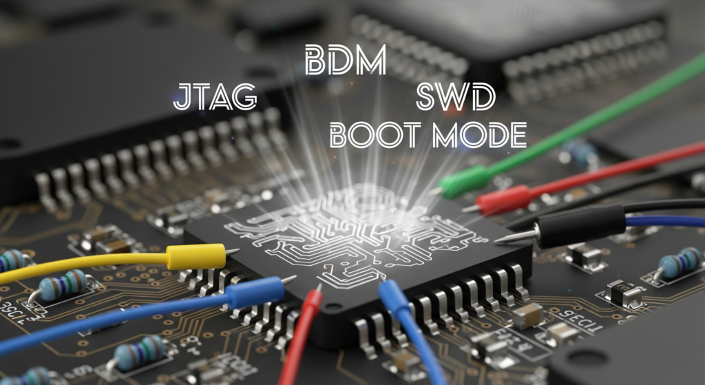
Modern automotive ECUs employ a range of microcontroller families Infineon Tricore, Freescale/NXP PowerPC, Renesas V850 and RH850, ST Microelectronics SPC5, and various ARM Cortex variants each with different debug and programming interfaces. The four primary extraction vectors JTAG, BDM, SWD, and boot mode each exploit different hardware capabilities of these microcontrollers.
This guide provides a thorough, comparative analysis of each method, with practical guidance on hardware requirements, security implications, and the real-world scenarios where each approach excels.
Why ECU Firmware Extraction Matters
Before diving into the technical methods, it is worth framing why firmware extraction is performed:
- Calibration analysis and tuning: Extracting the firmware to examine or modify fuel maps, ignition timing tables, boost targets, torque limiters, and other calibration parameters
- Security research: Analyzing the ECU’s security implementation including seed-key algorithms, immobiliser protocols, secure boot chains, and cryptographic implementations
- Forensic investigation: Obtaining an unmodified firmware image for legal proceedings, insurance disputes, or emissions compliance verification
- Failure analysis: Diagnosing ECU malfunctions by examining firmware state, adaptive learning values, and fault memory contents
- Interoperability and aftermarket development: Understanding communication protocols and data structures for developing diagnostic tools or aftermarket accessories
Each of these use cases may favor different extraction methods based on the required completeness of the dump, the need to preserve the ECU’s operational state, and the acceptable level of physical invasiveness.
JTAG (Joint Test Action Group) IEEE 1149.1
Technical Overview
JTAG is arguably the most versatile and powerful debug interface available on automotive microcontrollers. Originally developed as IEEE 1149.1 for boundary-scan testing of PCB solder joints, JTAG evolved into the predominant on-chip debug interface for embedded processors. In the automotive ECU context, JTAG provides full read/write access to the processor’s memory space, including flash memory, RAM, and peripheral registers.
The JTAG interface uses a minimum of four signal lines:
| Signal | Function |
|---|---|
| TCK | Test Clock synchronizes all JTAG operations |
| TMS | Test Mode Select navigates the JTAG state machine |
| TDI | Test Data In serial data input to the target |
| TDO | Test Data Out serial data output from the target |
| TRST (optional) | Test Reset asynchronous reset of the JTAG TAP controller |
These signals implement a serial protocol governed by the TAP (Test Access Port) state machine defined in the IEEE 1149.1 standard. Through this interface, a debug probe can halt the processor, read and write memory, set breakpoints, and single-step through code execution.
JTAG in Automotive ECU Context
Different microcontroller families implement JTAG with varying extensions:
- Infineon Tricore (Bosch MED17/EDC17): Implements OCDS (On-Chip Debug Support) over a JTAG-compatible interface. Tricore extends standard JTAG with the Cerberus debug module, providing hardware breakpoints, trace capabilities, and direct memory access. The Tricore DAP (Device Access Port) interface is a compact 10-pin or smaller debug connector variant.
- Freescale/NXP MPC5xxx (Bosch ME7, some Continental ECUs): Uses the Nexus debug standard (IEEE-ISTO 5001) which is accessed through JTAG but provides additional capabilities including real-time data trace and program trace through auxiliary output pins.
- Renesas V850/RH850 (Denso ECUs): Implements JTAG with Renesas-specific extensions including the E1/E2 debug interface protocols. The physical connector varies but the underlying protocol remains JTAG-based.
- ARM Cortex-based ECUs (newer Continental, Bosch, Delphi units): ARM processors implement CoreSight debug architecture, accessed through either JTAG or the newer SWD interface (discussed separately below).
Hardware Requirements
Professional JTAG extraction requires:
- Debug probe: The industry standard for automotive work is the Lauterbach TRACE32 system, which provides the broadest processor support and most reliable operation. Alternatives include PLS UDE (Universal Debug Engine), iSYSTEM winIDEA, and Segger J-Link (primarily for ARM targets). For Tricore specifically, the Lauterbach PowerDebug interface with a Tricore-specific license is the gold standard.
- Target connection: Physical connection to the JTAG pins on the ECU PCB. This typically requires identifying the JTAG test points on the board (which may be unpopulated pads, vias, or removed connectors) and soldering fine-gauge wires or using spring-loaded pogo pin adapters.
- Power supply: The ECU must be powered during extraction, either on the bench with a suitable power supply simulating the vehicle’s electrical system, or in-vehicle.
- Level shifting (if needed): Most automotive ECUs use 3.3 V or 5 V logic levels. The debug probe must match the target voltage. Professional probes handle this automatically; lower-cost adapters may require external level shifting.
Extraction Procedure (General)
- Identify the JTAG test points on the ECU PCB through visual inspection, continuity testing to known processor pins, or reference to available board documentation
- Make secure physical connections to TCK, TMS, TDI, TDO, and GND (plus TRST if available)
- Power up the ECU and establish communication with the debug probe software
- Configure the debug probe for the correct processor type and clock speed
- Halt the processor (if required by the probe software)
- Read the memory regions of interest typically the entire PFLASH, DFLASH, and optionally RAM contents
- Save the dump to file and verify integrity by re-reading and comparing
Security Considerations
JTAG security is the primary obstacle in modern ECU extraction:
- JTAG password/lock: Many Tricore-based ECUs set the OCDS password during manufacturing, preventing unauthorized debug access. Without the correct password, the JTAG interface rejects connection attempts. Recovery of the OCDS password may require alternative extraction methods (boot mode) or exploitation of silicon-level vulnerabilities.
- Permanent JTAG disable: Some security-critical ECUs permanently disable the JTAG interface by blowing fuses (OTP bits) during manufacturing. Once disabled, JTAG access cannot be restored through software means.
- Debug authentication: ARM CoreSight implements authenticated debug access on some variants, requiring cryptographic authentication before granting debug privileges.
When to Use JTAG
JTAG is the preferred method when:
- You need a complete firmware dump including bootloader, application, and data flash
- You require live debugging capability (breakpoints, memory watch, register inspection)
- The JTAG interface is accessible and not locked
- You are performing security research that benefits from runtime analysis
- You need to recover a bricked ECU by reflashing via JTAG
BDM (Background Debug Mode)
Technical Overview
BDM is a debug interface specific to the Freescale/NXP (formerly Motorola) microcontroller families, most notably the 68HC12, HCS12, MPC5xx, and MPC55xx series. In the automotive ECU world, BDM is primarily associated with older Bosch ECU platforms (ME7.x, MSA15, MS6, and others using Motorola/Freescale processors) and certain Continental and Siemens ECU families.
BDM operates through a single bidirectional data line (BKGD) plus a clock reference, making it physically simpler than JTAG. The BDM protocol allows the debug host to:
- Read and write CPU registers
- Read and write memory (including flash)
- Execute single instructions on the target processor
- Halt and resume program execution
- Erase and program flash memory
BDM Variants
Two distinct BDM implementations exist, and they are not interchangeable:
- HC12/HCS12 BDM: Single-wire synchronous protocol used on the 68HC12 and HCS12 microcontroller families. Common in older automotive ECUs from the early 2000s. The protocol operates at a fixed fraction of the target’s bus clock.
- PowerPC BDM (also called COP Common On-chip Processor debug): Used on the MPC5xx and MPC55xx families. This version operates over a JTAG-like multi-wire interface and is technically closer to JTAG than to HC12 BDM despite sharing the BDM name. The Freescale Nexus debug standard, accessed through this interface, provides program trace and data trace capabilities.
This naming overload causes frequent confusion. When someone refers to “BDM” in an automotive context, the meaning depends entirely on the target processor family.
Hardware Requirements
- BDM adapter: For HC12/HCS12 targets, common adapters include the Motorola/P&E TBDML, USBDM (open-source), and various commercial BDM interfaces. For MPC5xx/PowerPC targets, a Lauterbach TRACE32, PLS UDE, or P&E Multilink is typical.
- Target connection: HC12 BDM requires a single BKGD pin connection plus GND and reset. MPC5xx BDM/Nexus requires the multi-pin JTAG/Nexus connector. As with JTAG, these test points may need to be located on the ECU PCB.
BDM in the ECU Reverse Engineering Context
BDM was historically the primary extraction method for an entire generation of automotive ECUs. The Bosch ME7.x family (used in countless Volkswagen, Audi, BMW, and Porsche vehicles from approximately 1999–2008) used Siemens C16x/ST10 processors with a BDM-like on-chip debug interface. The famous “BDM read” of ME7 ECUs which enabled the first generation of serious aftermarket ECU tuning exploited these debug interfaces.
For Freescale-based ECUs (such as those used by Delphi, Continental, and some Bosch diesel controllers), the PowerPC BDM/Nexus interface provided similar firmware extraction capability.
Security Considerations
- HC12/HCS12: These older parts have relatively limited debug security. Some variants implement a security byte that disables BDM access, but well-known bypass techniques exist for most variants.
- MPC5xxx: Later PowerPC parts implement the Nexus censorship mechanism, which restricts debug access when security is enabled. Circumventing MPC55xx censorship is a well-documented challenge in the automotive reverse engineering community.
When to Use BDM
BDM is the appropriate choice when:
- The target ECU uses a Freescale/NXP HC12, HCS12, or MPC5xx processor
- You are working with older ECU platforms (pre-2010 era)
- The BDM interface is accessible on the PCB
- You need flash programming capability for the target microcontroller family
SWD (Serial Wire Debug)
Technical Overview
SWD is a two-pin debug interface developed by ARM as part of the CoreSight debug architecture. It provides equivalent functionality to JTAG but requires only two signal pins instead of four (or five). SWD was designed as a pin-count-optimized alternative to JTAG for ARM Cortex-M and Cortex-R processors.
The two SWD signals are:
| Signal | Function |
|---|---|
| SWDIO | Serial Wire Data I/O : bidirectional data line |
| SWCLK | Serial Wire Clock : clock signal driven by the debug probe |
SWD provides full debug access including:
- Read/write access to all memory-mapped resources
- Processor halt, resume, single-step
- Hardware and software breakpoints
- Real-time memory access without halting (through the DAP -Debug Access Port)
SWD in Automotive ECUs
ARM Cortex-based processors are increasingly common in automotive ECUs, particularly in:
- Body control modules (BCMs) and comfort electronics using Cortex-M series
- Newer engine management ECUs from Continental, Bosch, and others using Cortex-R or Cortex-A for ADAS integration
- Transmission control units (TCUs) using ARM-based controllers
- Infotainment and gateway ECUs using higher-end ARM processors
As ARM Cortex processors continue to gain market share in automotive applications, SWD is becoming an increasingly relevant extraction interface. However, for traditional powertrain ECUs (engine and transmission), Tricore and PowerPC still dominate the installed base.
Hardware Requirements
- Debug probe: The Segger J-Link is the most widely used SWD-capable debug probe, offering broad ARM Cortex support. The ST-Link (for ST Microelectronics targets), CMSIS-DAP compatible probes, and Lauterbach TRACE32 (with ARM support) are alternatives. The open-source Black Magic Probe is a capable low-cost option for ARM SWD.
- Target connection: Two signal wires (SWDIO, SWCLK) plus GND. Some implementations also use the SWO (Serial Wire Output) pin for trace data.
Security Considerations
ARM CoreSight implements several security features relevant to ECU extraction:
- Read-out protection (RDP): ARM Cortex-M microcontrollers from various vendors (STM32, NXP LPC, etc.) implement flash read-out protection at multiple levels. Level 1 typically prevents debug read access but can be disabled (with a full flash erase). Level 2 permanently disables debug access.
- TrustZone: ARM TrustZone technology partitions the processor into Secure and Non-Secure worlds. Debug access to the Secure world requires explicit authentication or is permanently disabled in production devices.
- Secure debug authentication: Some implementations require cryptographic authentication before granting debug access, similar to Tricore OCDS passwords but using certificate-based authentication.
When to Use SWD
SWD is the appropriate choice when:
- The target ECU uses an ARM Cortex-M, Cortex-R, or Cortex-A processor
- You need a pin-efficient debug connection (only 2 signals vs. JTAG’s 4-5)
- You are working with newer vehicle electronics using ARM-based controllers
- The SWD interface is not locked by read-out protection or secure debug
Boot Mode (Bootstrap Loader) Extraction
Technical Overview
Boot mode extraction exploits the factory-programmed bootstrap loader (BSL) present in the mask ROM of most automotive microcontrollers. This ROM code, burned into the silicon by the chip manufacturer, provides a minimal communication interface (typically UART or SPI) for initial flash programming during ECU manufacturing. By activating boot mode through specific hardware pin configurations during power-on reset, the BSL takes control instead of the normal firmware, providing external access to flash memory.
Boot mode is fundamentally different from JTAG, BDM, and SWD in that it does not use a debug interface. Instead, it leverages the chip manufacturer’s factory programming protocol. This distinction is important because boot mode access and debug interface access are controlled by separate security mechanisms.
Boot Mode Across Processor Families
Infineon Tricore (MED17/EDC17):
- Activated by configuring the HWCFG (Hardware Configuration) pins during reset
- BSL communicates over UART (ASC0 peripheral) at specific baud rates
- The Tricore BSL protocol supports flash read, flash write, flash erase, and jump-to-address commands
- Modern Tricore variants implement BSL password protection an 8-byte password must be supplied before the BSL grants access
Freescale/NXP MPC5xxx:
- Activated by the BAM (Boot Assist Module) when configured for serial boot
- Communicates over SCI (UART) or CAN
- The BAM protocol varies by MPC5xxx sub-family
Renesas V850/RH850:
- Activated through dedicated mode pins
- Uses a UART-based programming protocol
- Security features vary by variant
ST Microelectronics SPC5/STM32:
- STM32 devices have a well-documented system bootloader in ROM activated by the BOOT0 pin
- SPC5 devices have similar factory boot ROM capability
- ST’s bootloader protocol supports UART, SPI, I2C, and USB on various variants
Hardware Requirements
Boot mode extraction requires:
- USB-to-UART adapter: A standard FTDI FT232 or CP2102-based USB-to-UART adapter, level-shifted to match the target voltage (typically 3.3 V). For some protocols, a CAN interface may be used instead.
- PCB access: Physical connections must be made to the UART TX/RX pins of the microcontroller and to the hardware configuration pins that select boot mode entry. This typically requires soldering to specific test points or pads on the ECU PCB.
- Boot mode activation hardware: Resistors, jumper wires, or a custom adapter board to hold the mode selection pins at the correct logic levels during power-on reset.
- Protocol software: Custom scripts or tools that implement the BSL communication protocol. For Tricore, tools such as TriCore BSL Client and various open-source implementations exist. For STM32, STM32CubeProgrammer or the open-source stm32flash utility support the factory bootloader protocol.
The BSL Password Challenge
On modern Tricore-based ECUs (the majority of MED17/EDC17 variants produced since approximately 2010), the BSL requires a correct 8-byte password before granting any access. This password is typically derived from the flash contents or programmed during manufacturing. Without the correct password, the BSL will not respond to read or write commands.
BSL password recovery is an active area of automotive security research. Approaches include:
- Extracting the password from a partial firmware dump obtained through another method
- Exploiting timing-based or power-analysis side-channel vulnerabilities in the password verification routine
- Leveraging known relationships between the BSL password and other accessible ECU data
When to Use Boot Mode
Boot mode extraction is the appropriate choice when:
- The JTAG/debug interface is locked and cannot be bypassed
- You need a relatively non-invasive physical extraction method (compared to chip-off techniques)
- The target processor’s BSL is accessible and not password-protected (or the password is known)
- You are working with a processor family where boot mode provides complete flash access (not all do some BSL implementations restrict which memory regions can be read)
- Cost is a constraint boot mode requires only a basic UART adapter rather than an expensive professional debug probe
Unsure which extraction method is right for your ECU? Our engineers can assess your target and recommend the optimal approach. Get a free consultation →
Comparison Table: JTAG vs. BDM vs. SWD vs. Boot Mode
| Feature | JTAG | BDM | SWD | Boot Mode |
|---|---|---|---|---|
| Primary processor families | Tricore, PowerPC, ARM, most others | Freescale HC12, HCS12, MPC5xx | ARM Cortex-M/R/A | All (processor-specific BSL) |
| Signal count | 4–5 (TCK, TMS, TDI, TDO, TRST) | 1 (HC12) or 4+ (PowerPC) | 2 (SWDIO, SWCLK) | 2–3 (UART TX, RX, mode pin) |
| Flash read | Yes | Yes | Yes | Yes (if not password-locked) |
| RAM read | Yes | Yes | Yes | Limited or no |
| Live debugging | Yes | Yes | Yes | No |
| Breakpoints | Yes | Yes | Yes | No |
| Real-time trace | Some implementations | Nexus variants | SWO/ETM variants | No |
| Typical read speed | Fast (MB/min range) | Moderate | Fast | Slow to moderate |
| Hardware cost | High ($1K–$15K for professional probes) | Moderate ($50–$5K) | Low to moderate ($20–$5K) | Low ($10–$30 UART adapter) |
| Physical invasiveness | Moderate (solder to test points) | Moderate (solder to test points) | Low to moderate | Moderate (solder to test points + mode pins) |
| Common security obstacles | JTAG password, fuse-blown disable | Censorship bits, security byte | RDP levels, secure debug | BSL password, restricted regions |
| Dump completeness | Full (all memory regions) | Full (all memory regions) | Full (all memory regions) | Varies (may exclude bootloader or protected regions) |
| ECU state preservation | Can be non-destructive | Can be non-destructive | Can be non-destructive | Requires reset into boot mode |
OBD-Based Extraction: The Fifth Method
While not a hardware debug interface, OBD-based firmware extraction deserves mention as a practical method used extensively in the tuning community. This approach uses the ECU’s own diagnostic communication interface the OBD-II port connected via CAN, K-Line, or other vehicle bus protocols to read firmware data through diagnostic services.
How It Works
OBD-based extraction typically leverages:
- UDS Service 0x23 (ReadMemoryByAddress): After successful SecurityAccess (Service 0x27) authentication, this standard UDS service allows reading arbitrary memory addresses from the ECU. The seed-key algorithm for the SecurityAccess challenge must be known or reverse engineered.
- Bootloader flash update protocol exploitation: By initiating a firmware update session and manipulating the protocol, some tools can extract the existing firmware rather than (or in addition to) writing new firmware.
- Manufacturer-specific extended services: Some ECU platforms implement non-standard diagnostic services that provide memory read capabilities.
Advantages of OBD-Based Extraction
- No ECU removal required extraction can be performed through the vehicle’s OBD-II port
- No soldering or PCB work completely non-invasive physically
- Fast and repeatable once the protocol is understood, extraction takes minutes
- Preserves ECU state no boot mode reset or debug halt required
Limitations
- Seed-key dependency: Requires knowledge of the SecurityAccess algorithm, which is manufacturer- and ECU-specific
- Incomplete dumps: The bootloader region and certain protected memory areas are typically inaccessible via OBD
- Protocol knowledge required: Each ECU family uses different diagnostic protocols and addressing schemes
- Not universal: Some ECUs do not expose ReadMemoryByAddress or restrict it to narrow address ranges even after SecurityAccess
Choosing the Right Extraction Method: Decision Framework
Selecting the optimal extraction method depends on several factors. Here is a practical decision framework:
Step 1: Identify the Target Processor
The processor family immediately narrows your options:
- Tricore → JTAG (OCDS) or Boot Mode (BSL)
- Freescale HC12/HCS12 → BDM
- Freescale MPC5xxx → BDM/Nexus (via JTAG connector) or Boot Mode
- ARM Cortex → SWD or JTAG
- Renesas V850/RH850 → JTAG or Boot Mode
Step 2: Assess Debug Interface Accessibility
Physically locate the debug interface test points on the ECU PCB. Are they accessible? Are they protected (potted in epoxy, covered by shielding)? The physical accessibility may eliminate certain options.
Step 3: Evaluate Security Status
Is the debug interface locked? Is boot mode password-protected? Has the JTAG been permanently disabled via fuses? The security status of each interface determines which options are viable.
Step 4: Define Your Requirements
- Need live debugging? → JTAG, BDM, or SWD (boot mode cannot do this)
- Need a complete dump including bootloader? → JTAG, BDM, or SWD (boot mode and OBD typically do not provide this)
- Minimal equipment budget? → Boot mode (UART adapter) or OBD-based
- Cannot remove the ECU from the vehicle? → OBD-based extraction
- Forensic evidence integrity? → JTAG or BDM with documented chain-of-custody procedures
Step 5: Consider Multi-Method Approaches
In practice, complex reverse engineering projects often combine multiple extraction methods. For example:
- OBD read to obtain the application and calibration data non-invasively
- Boot mode or JTAG to obtain the complete dump including bootloader for security analysis
- JTAG live debug to analyze runtime behavior and security mechanism implementation
Post-Extraction: Verifying Your Dump
Regardless of the extraction method used, verifying the integrity of your firmware dump is a critical step often overlooked by inexperienced practitioners.
Verification Techniques
- Multiple reads and comparison: Perform the extraction at least twice and compare the resulting binaries byte-for-byte. Any differences indicate a communication error, a read timing issue, or a non-static memory region.
- Known pattern verification: Check for expected patterns at known offsets Tricore firmware should have a valid Boot Mode Header (BMHD) at the start of PFLASH, ARM firmware should have a valid vector table, etc.
- Entropy analysis: A valid firmware dump will show characteristic entropy patterns code regions with moderate-high entropy, data/calibration regions with lower entropy, and unused/erased regions filled with 0xFF bytes showing zero entropy.
- Checksum verification: If the firmware’s internal checksum structure is known, verify that the checksums are consistent with the dump contents. A valid dump should have matching checksums; a corrupted dump likely will not.
For an in-depth treatment of checksum verification techniques, see our guide on ECU Checksum & CRC Algorithms.
Real-World Scenarios
Scenario 1: Extracting a Bosch MED17.5.2 (VW/Audi 2.0 TFSI)
Processor: Infineon TC1766
Available interfaces: JTAG (OCDS password protected), Boot Mode (BSL password protected), OBD (SecurityAccess required)
Approach: OBD-based extraction using a known seed-key algorithm for the application firmware, followed by boot mode extraction using a recovered BSL password for the complete dump including bootloader.
Scenario 2: Forensic Analysis of a Bosch EDC17C46 (Diesel Emissions Investigation)
Processor: Infineon TC1797
Requirement: Complete, forensically sound firmware dump with documented extraction methodology
Approach: JTAG extraction using Lauterbach TRACE32 with photographed and documented connection points. Multiple reads performed and hashed (SHA-256) for evidence integrity. Boot mode extraction performed separately as corroboration.
Scenario 3: Recovering a Bricked Continental SID807 (Peugeot/Citroën)
Processor: ST SPC560P
Situation: ECU non-functional after a failed flash update
Approach: JTAG extraction to read the current (partially corrupted) flash state, followed by JTAG-based reflash of a known-good firmware image to recover the unit.
Conclusion
ECU firmware extraction is both a science and a craft. The four primary hardware interfaces JTAG, BDM, SWD, and boot mode each serve different processor families and offer distinct capability profiles. JTAG remains the most universally capable interface, providing full debug and memory access where available. BDM serves the legacy Freescale ecosystem that underpins a large installed base of automotive ECUs. SWD is the rising interface tracking the adoption of ARM Cortex processors in automotive applications. Boot mode provides a fallback extraction path when debug interfaces are secured, using the chip manufacturer’s own factory programming protocol.
The practical reality of ECU reverse engineering is that no single method covers all scenarios. A well-equipped lab maintains tooling for all four interfaces, supplemented by OBD-based extraction capabilities, and selects the optimal approach based on the specific target ECU, its security configuration, and the objectives of the analysis.
Need reliable firmware extraction from any ECU platform? Our lab is equipped with Lauterbach TRACE32, PLS UDE, Segger J-Link, and custom boot mode tooling covering Tricore, PowerPC, ARM, Renesas, and ST Micro targets. From bench reads to forensic-grade extractions, we have the equipment and expertise. Contact reverseengineer.net today →
Let's Work Together
Need Professional Assistance with Reverse Engineering or Cybersecurity Solutions? Our Team is Ready To Help You Tackle Complex Technical Challenges.